WireWorld Gates and Gadgets


Requires a Wolfram Notebook System
Interact on desktop, mobile and cloud with the free Wolfram Player or other Wolfram Language products.
At each step in the WireWorld cellular automaton, background cells go to background, electron heads go to electron tails, electron tails go to wire, and wire goes to either wire or head, the latter when the wire cell touches one or two electron head cells. Electrical circuits can be modeled with WireWorld.
[more]
Contributed by: Karl Scherer (September 2013)
Additional contributions by: Bryan Silverman (who invented WireWorld), Nyles Heise, Matthieu Walraet, David Moore, Mark Owen, Michael Greene, Klaus Mogensen, and Tony Ennis
Open content licensed under CC BY-NC-SA
Snapshots

Details
You can click the board anywhere to modify the presented diagram.
If clicked repeatedly, a square of background color will turn yellow, then red, then blue, then back to background color.
Diagrams
Diagram 1-1: DIODE A diode or "one-way gate" lets the electrons through only in one direction and blocks all electrons moving in the opposite direction.
Diagram 1-2: TRANSISTORS A "transistor" (as we use the term here) allows on/off control of a current by an external signal. Click button "6" repeatedly to create several cycles. The "electron guns" or "clocks" on the left emit an electron at regular intervals.
Top diagram: "Negative Transistor" : ANDNOT gate = AND(A, NOT(B)) The negative transistor lets the current pass whenever the "base" (control contact) has no electrons coming in. (Note that this is opposite to the behavior of a real transistor in electronics.) See also the special variant on ANDNOT gates for more information.
Bottom diagram: "Positive Transistor" : AND gate The positive transistor lets the current pass whenever the "base" (control contact) has electrons coming in. Note that this is the behavior of a real transistor in electronics. Alternatively, we could have used a negative transistor plus a NOT gate to create a positive transistor (AND gate), but our construction given here is much simpler.
See also the special diagrams on AND gates for more information.
The loops at the left that spit out electrons at regular intervals are called "clocks".
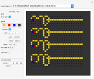
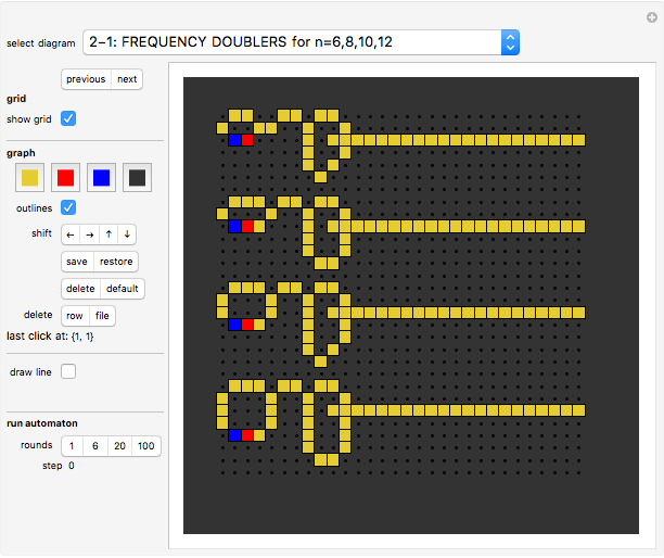
Diagram 2-1: FREQUENCY DOUBLERS double the clock rate.
Diagram 2-2: FREQUENCY HALVERS delete every second electron.
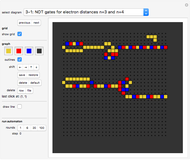
Diagrams 3-1, 3-2, 3-3: NOT gates A NOT gate spits out data (here WireWorld electrons) whenever there is NO input. The WireWorld electrons have to be regularly spaced (timed) for the NOT gates to work.
Diagram 4-1: ANDNOT gate for any  . Design by Michael Greene.
The right end of the wire receives an electron if the bottom input wire (but not the top input wires) has data.
. Design by Michael Greene.
The right end of the wire receives an electron if the bottom input wire (but not the top input wires) has data.
Diagram 4-2: ANDNOT gates for  . Designs by Nyles Heise.
Diagram 4-3: ANDNOT gate for any  .
.
Diagram 5-1: OR gate.
The right end of the wire receives an electron if one or both of the two input wires has data. The gate design works for all . A NOR gate can be constructed from an OR gate followed by a NOT gate.
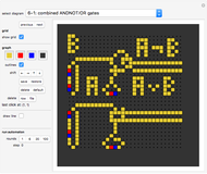
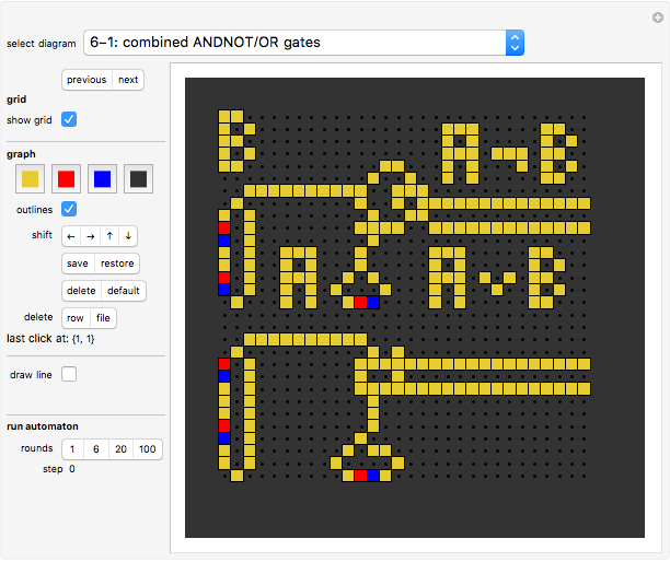
Diagram 6-1: combined ANDNOT/OR gates.
Top: Design by Klaus Mogensen. Works for  .
Bottom: Design by David Moore and Mark Owen. Works for .
.
Bottom: Design by David Moore and Mark Owen. Works for .
Diagram 7-1: XOR gate for all .
The right end of the wire receives an electron if one or both of the two input wires has data.
Design by Michael Greene.
XOR stands for "exclusive or", meaning "create output data if either input is active, but not if both are active".
The XOR shown here is built from other components using the fact that XOR(A,B) = ((A and not B) or (B and not A)).
Diagram 7-2: Two XOR gates for .
Design by Nyles Heise. Note that the top one works for all !
The underscored "V" sign at the top is the sign for the logical "XOR".
Diagram 7-3: XOR gates for .
Left: XOR gates for any , design by Mathieu Walraet. The gate works for all . Its symmetry allows it to emit the result to BOTH sides.
Center: Well-known XOR for  or larger. Right: XOR for
  by Karl Scherer.
Diagram 8-1: AND gate for  .
Design by Nyles Heise and Karl Scherer.
An AND gate sends an electron to the output wire whenever there is an electron arriving at both input wires.
The design for 3-tick data presented here uses OR and NOT gates:
AND (A,B) = NOT (NAND(A,B)) = NOT ((NOT(A) OR NOT(B))
Note that 6-cycle gates have been used here to build the 3-cycle gate.
.
Design by Nyles Heise and Karl Scherer.
An AND gate sends an electron to the output wire whenever there is an electron arriving at both input wires.
The design for 3-tick data presented here uses OR and NOT gates:
AND (A,B) = NOT (NAND(A,B)) = NOT ((NOT(A) OR NOT(B))
Note that 6-cycle gates have been used here to build the 3-cycle gate.
Diagram 8-2: AND gate for . Design by Nyles Heise.
Diagram 8-3: AND gates for any . Designs by Karl Scherer based on older sub-optimal designs.
Diagram 8-4: AND gate for any . Design by Nyles Heise.
Diagram 8-5: AND gates for any  . Designs by Nyles Heise (top) and Karl Scherer (bottom). Both diagrams are based on AND(A,B) = AND(A, ANDNOT(NOT (B))).
Diagram 9-1: NAND gate for . Design by Nyles Heise.
A NAND gate always sends an electron except when both input wires have data.
This is based on the fact that (NAND(A,B)= OR(NOT(A),(NOT(B)).
Note that 6-cycle gates have been used here to build the 3-cycle gate.
Diagram 9-2: NAND gate for . Design by Karl Scherer and Nyles Heise.
Diagram 9-3: NAND gates for .
Top: Design by Karl Scherer. Bottom-right: Widely published version.
Diagram 9-4: NAND gates for .
Top: Designs by Karl Scherer. Bottom: widely published.
Diagram 10-1: EQUAL gates for .
Design by Karl Scherer. Bottom: widely published.
The EQUAL gate fires when both input lines or neither of them carry an electron.
Diagram 11-1: WIRE CROSSING for .
Design by Michael Greene; slightly improved by Karl Scherer.
Diagram 11-2: WIRE CROSSING for .
Design by Nyles Heise.
Diagram 11-3: WIRE CROSSING for any .
Design by Klaus Mogensen.
Diagram 11-4: WIRE CROSSINGs for any .
All are based on the fact that (B XOR (A XOR B)) = A, (A XOR (A XOR B)) = B.
Left: Widely publicized, but not the smallest crossing. Works for all .
Right: Design by Karl Scherer; smaller, works for all .
Bottom: Design by Karl Scherer; works for all .
Diagram 11-5: WIRE CROSSING for .
Design by Karl Scherer.
Diagram 12-1: ASYNCHRONOUS WIRE CROSSING for .
Design by David Moore and Mark Owen.
Asynchronous wire crossings need the electrons in the two data streams not to arrive at the same time (in our example we have (A,B) => ((A andnot B),(B andnot A)).
Diagram 12-2: special WIRE CROSSING (A,B)=>(A AND B, A), for .
Design by Karl Scherer.
Diagram 13-1: FUSE for .
The fuse lets the first electron pass and stops all other electrons.
Diagram 14-1: ROM (read-only memory) for .
Design by David Moore and Mark Owen.
Several combined ANDNOT/OR gates can be arranged in a rectangular pattern to form a read-only memory. Here we have three input ("read") lines, each associated with three stored bits. Each "read electron" can trigger several output lines. The stored bits are those gates that have a missing "ear".
Diagram 15-1: three-cycle mono-input FLIP-FLOP by Karl Scherer.
Once triggered by an incoming electron, a mono-input flip-flop spits out electrons non-stop until a second electron arrives.
Diagram 15-2: three-cycle mono-input FLIP-FLOP by Nyle Heise.
Diagram 15-3: mono-input FLIP-FLOPS for  .
Designs by Nyles Heise.
.
Designs by Nyles Heise.
Diagram 15-4: more mono-input FLIP-FLOPS for  .
Designs by Karl Scherer.
.
Designs by Karl Scherer.
Diagram 15-5: mono-input FLIP-FLOPS for  .
Designs by Karl Scherer, based on Nyles' diagrams for
.
Designs by Karl Scherer, based on Nyles' diagrams for
Diagram 15-6: more mono-input FLIP-FLOPS for .
Designs by Karl Scherer.
Diagram 15-7: special mono-input FLIP-FLOPS for  .
The flip-flop by Karl Scherer shown on top is the only one known for 5-tick data.
Since there is no 5-tick loop in WireWorld, a 10-tick loop with two electrons has been used instead.
The 7-cycle flip-flop shown here is the smallest mono-input flip-flop overall.
It consists of only 13 cells and was found by Matthieu Walraet.
.
The flip-flop by Karl Scherer shown on top is the only one known for 5-tick data.
Since there is no 5-tick loop in WireWorld, a 10-tick loop with two electrons has been used instead.
The 7-cycle flip-flop shown here is the smallest mono-input flip-flop overall.
It consists of only 13 cells and was found by Matthieu Walraet.
Diagram 16-1: dual-input FLIP-FLOP for .
Design by Michael Greene.
Dual-input FLIP-FLOPs are also called "RS-latches" (reset/set latches). An electron in the top input line starts the flip-flop, and an electron in the bottom input line stops it. If both lines carry an electron, the start-signal is ignored; this latch is "reset-dominant".
Diagram 16-2: dual-input FLIP-FLOP for .
Reset-dominant RS-latch by Nyles Heise.
Diagram 16-3: dual-input FLIP-FLOP for .
Set-dominant RS-latch by Karl Scherer.
Diagram 16-4: dual-input FLIP-FLOP for .
Reset-dominant RS-latch.
Diagram 17-1: REFLECTOR. A reflector inverses the direction of an electron's move.
Diagram 17-2: fun application of a REFLECTOR. After a boring start, the display gets quite wild.
Diagram 18-1: positive EDGE DETECTORS for  .
Of several arriving electrons, this gate only lets the first one pass.
.
Of several arriving electrons, this gate only lets the first one pass.
Diagram 18-2: negative EDGE DETECTORS for  .
This gate send a signal when it detects the first zero after a sequence of electrons; e.g. it turns 111001011000... into 000100100100.... Top: ; bottom: .
.
This gate send a signal when it detects the first zero after a sequence of electrons; e.g. it turns 111001011000... into 000100100100.... Top: ; bottom: .
Diagram 18-3: TWO-EDGE DETECTORS for .
A two-edge detector sends one electron when the input bit string starts and one electron when it ends.
Diagram 18-4: reconstructing a data string from its edges.
Diagram 19-1: delete the third electron in a continuous data stream ().
Diagram 20-1: 001-DETECTOR ().
Fires if it detects two zeros followed by a 1. Design by Karl Scherer.
Diagram 20-2: 010-DETECTOR ().
Design by Karl Scherer.
Fires if it detects an isolated electron (top output line).
Here used to delete isolated electrons from the data stream (bottom output line).
Diagram 20-3: GAP-FILLER ().
Replaces any 101 pattern with a 111 pattern. Design by Karl Scherer.
Diagram 21-1: DATA-SPLITTER (de-multiplexer), .
Every datum in the input stream (0 or 1) is directed alternatingly to one of two output streams. Design by Karl Scherer.
Diagram 21-2: DATA-SPLITTERS (de-multiplexers),  .
.
Diagram 21-3: controlled DATA-SPLITTER, .
The input stream (from left) is directed to one of two output lines.
Without control input (from the top), the stream is directed to the top output line; otherwise, it is directed to the bottom output line. Design by Karl Scherer.
Diagram 21-4: controlled DATA-SPLITTER, . Design by Karl Scherer.
Diagram 21-5: data-driven DATA-SPLITTER, . Design by Karl Scherer.
Every arriving electron ends up on an output line different from the last electron's output line.
Diagram 21-6: data-driven DATA-SPLITTER, . Design by Karl Scherer.
Diagram 22-1: controlled MULTIPLEXER, . Design by Karl Scherer.
Diagram 23-1: lengthening and shortening of bit strings, n=5. Design by Karl Scherer.
Diagram 23-2: lengthening and shortening of bit strings, n=6. Design by Karl Scherer.
Diagram 24-1: BINARY ADDER, . Design by Klaus Mogensen. Setup: 3+5=8.
Diagram 24-2: BINARY ADDER, . Design by Klaus Mogensen. Setup: 3+5=8.
Diagram 24-3: BINARY ADDER, . Design by Tony Ellis. Setup: 3+5=8.
Diagram 24-4: BINARY ADDER, again. Design by Klaus Mogensen. Setup: 3+5=8.
Diagram 24-5: BINARY ADDER, once more. Design by David Moore and Mark Owen. Setup: 3+1=4.
The top input is copied undisturbed for convenience. It helps to find the position of the lowest digit in the output of the binary adder.
"previous/next" buttons Go to the previous/next diagram.
"show grid" checkbox Show/hide the 30×30 grid of dots.
Four color swatches Here you can change the WireWorld colors.
"outlines" checkbox Display the rims of the small squares.
"shift" buttons Shift the diagram in one of the four main directions.
"save/restore" buttons
Save/restore the current diagram.
"delete/default" buttons
Delete the current diagram or reset the diagram to default.
"delete row/file" buttons
Delete the row or file that was clicked last. The coordinates of the point clicked last are displayed.
"draw line" checkbox
You can easily draw additional wiring with the line drawing mode.
Check the box to enter line drawing mode.
Note: do not click any other buttons when in line drawing mode!
When in drawing mode, first click the board to mark the start position of the yellow line you want to draw (an orange dot will mark the position), then click the board to mark the end of the line (the line will be drawn automatically). The second click must be positioned in the same row, file, or diagonal as the first click.
Uncheck the box to leave line drawing mode.
"rounds 1/6/20/100" buttons
Run the WireWorld diagram for 1/6/20/100 steps. A step counter is displayed.
History
All WireWorld gates and gadgets displayed in this Demonstration have been published before by the same author as the Zillions game "Wireworlds".
Permanent Citation
 String Matching Automaton
Michael Schreiber Balanced Annihilation
Michael Schreiber Elementary Cellular Automaton Egg
Michael Schreiber 2D Totalistic Cellular Automata
Luca Zammataro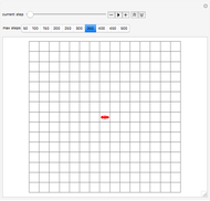 Grid Designs Generated by Langton's Ant
Rohith Kodukula Representing an Integer with an Elementary Automaton
Michael Schreiber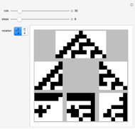 Semi-Rotation Automaton Plot
Michael Schreiber Coevolving Complements
Michael Schreiber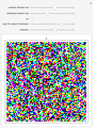 Totalistic Diffusion Elementary Reaction Automata
Michael Schreiber Reversible Multiplex of Totalistic Cellular Automata
Michael Schreiber
-
 Polyhedral Playground
Karl Scherer -
 Tiling Constructor, Tile-Dragging Variant
Karl Scherer -
 The Catenax Puzzle
Karl Scherer -
 Angel Puzzle
Karl Scherer -
 Constructing and Manipulating Graphs
Karl Scherer -
 3D Construction Set
Karl Scherer -
 Blended Quadrilaterals
Karl Scherer -
 Rotating Polyhedra in Space
Karl Scherer -
 The Misdirection Game
Karl Scherer -
 Tensegrity
Karl Scherer -
 Nowhere-Neat Tilings
Karl Scherer -
 Pocket Calculator
Karl Scherer -
 Area Puzzle
Karl Scherer -
 Molecule Construction Set
Karl Scherer -
 The Ray Puzzle
Karl Scherer -
 Animated Model of an Industrial Robot Arm
Karl Scherer -
 Model of an Industrial Robot Arm
Karl Scherer -
 Color-Blended Circular Tiles
Karl Scherer -
 Rep-Tiles
Karl Scherer -
 Armed Balloons Puzzle
Karl Scherer